Against the backdrop of the deep integration of Industry 4.0 and personalized manufacturing, the customized service of hardware stamping parts is evolving from single – part processing to system – level solutions. Based on the data from the 2025 industry technology white paper, this article analyzes the technological innovation paths and application practices of hardware stamping parts, providing a technical decision – making framework for the manufacturing industry.
I. Innovation in Materials Engineering: From General – purpose to Functional Customization
The performance breakthrough of hardware stamping parts begins with the scenario – based reconstruction of the material system:
High – strength and lightweight solutions
In the new energy vehicle field, DP1180 dual – phase steel is used, with a tensile strength of 1800MPa, achieving a 30% weight reduction of structural parts.
For smart wearable devices, titanium – nickel shape – memory alloy is applied, enabling 0.1 – mm – level deformation control of flexible circuit board brackets.
Functional composite materials
For 5G base – station shielding covers, copper – polyimide laminated stamping parts are used, increasing the electromagnetic shielding effectiveness to 120dB.
For medical surgical instruments, antibacterial stainless – steel stamping parts are used, and the silver – ion coating on the surface achieves a 99.99% bacteriostatic rate.
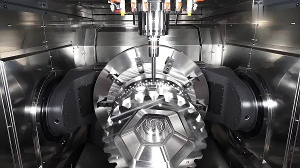
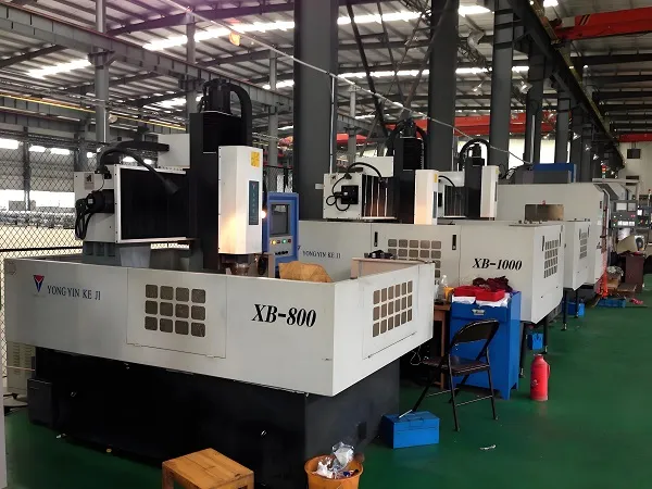
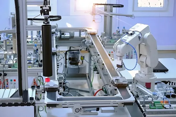
II. Reconstruction of the Precision Process Chain: Technological Breakthroughs and Efficiency Revolution
Based on the process databases of global leading enterprises, modern hardware stamping forms three major technical matrices:
Intelligent Mold System
Modular combined molds support the rapid switching of materials with a thickness of 0.2 – 8mm, and the model – changing time is compressed to 3 minutes.
The service life of nano – coated molds exceeds 5 million stamping strokes, reducing maintenance costs by 40%.
Dynamic Forming Control
Servo – motor – driven technology enables stepless adjustment of the stamping speed from 0.01 – 1500mm/s, and the forming accuracy of complex curved surfaces is ±0.015mm.
The laser – assisted positioning system compensates for material springback, controlling the debugging reject rate within 0.2%.
Composite Processing Technology
The stamping – tapping integrated process reduces process transfers by 70%, typically applied in the production of electronic connectors.
Micro – connection technology (Micro Joint) enables the automatic sorting of progressive dies, increasing efficiency by 45%.
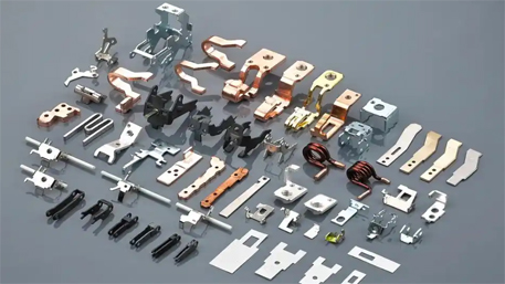
III. Industry – specific Deep – customization Solutions
New Energy Vehicle Electronic control system
For motor terminals, 0.08 – mm ultra – thin phosphor – bronze strips are stamped, increasing the conductivity to 85%IACS.
For high – voltage connectors, multi – station precision die technology is applied, with the contact resistance fluctuation ≤ 2%.
Core components of smart home appliances
For the stainless – steel stamping parts of dishwasher pumps, the deep – drawing process is used, with a drawing ratio breaking through 3:1.
The dust – box components of robotic vacuum cleaners go through 18 precision stamping processes, achieving an IP68 – level sealing performance.
Industrial automation equipment
The flexible wheel of the robot harmonic reducer uses the progressive stamping hardening technology, with a fatigue life of over 30,000 hours.
For the shell of the PLC controller, the mirror stamping process is applied, with a surface roughness Ra ≤ 0.05μm.
IV. Digital Quality System: From Process Control to Predictive Maintenance
Cloud Optimization of Process Parameters
The AI model trained based on millions of stamping data automatically generates the best pressure – speed curve, shortening the debugging cycle by 85%.
Deformation Prediction System
By integrating material phase analysis data, it can predict the springback of complex structural parts, with a compensation accuracy at the 0.008 – mm level.
Mold Health Monitoring
The vibration spectrum analysis system can issue an early warning of abnormal mold wear 72 hours in advance, reducing the unexpected downtime rate by 90%.
V. Future Technology Roadmap
Breakthroughs in Green Manufacturing
Biodegradable stamping oil agents achieve zero VOC emissions, reducing the water consumption in the cleaning process by 80%.
The waste AI sorting system increases the metal recovery rate to 99.6%.
Integration of Digital Twin
The process simulation system can simulate the mold deformation trend after tens of millions of stampings.
Blockchain technology enables full – process data tracing, supporting second – level traceability for quality disputes.
Empowerment Path of Customized Services
Leading enterprises build competitive advantages through three core capabilities:
Agile development system: Deliver rapid samples within 72 hours, supporting a minimum order quantity of 100 pieces.
Interdisciplinary engineering team: Integrate materials, mechanical, and electronic engineers to provide system – level solutions.
Digital service platform: Automatically generate process analysis reports and cost estimates by uploading drawings online.
(Note: The technical parameters in this article are quoted from the “2025 Global Stamping Technology White Paper” and industry – verified data. The implementation plan needs to be demonstrated in combination with specific working conditions.)