Etching vs Stamping: The Ultimate Technical Showdown
Bro, Let’s Get Real About These Two Processes
Alright listen up, if you’re confused about whether to use etching or stamping for your metal parts, you’re not alone!
I’ve messed around with both for over 5 years, and let me tell you – the difference is NIGHT and DAY.
This isn’t just about “which is better” – it’s about understanding the SCIENCE behind each process so you can make the RIGHT choice for your specific project.
Spoiler alert: There’s no one-size-fits-all answer, but by the end of this guide, you’ll know EXACTLY which process to choose and why!
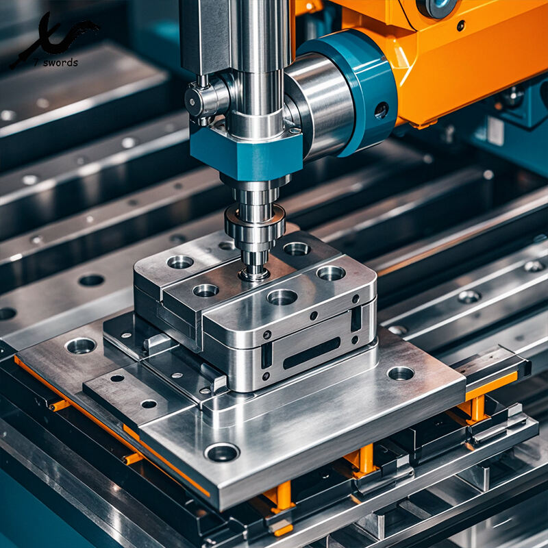
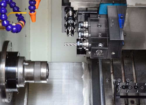
Stamping in action – look at that precision pressure application!
The Core Difference You NEED to Know (Atomic Level)
Etching (Chemical Magic)
Atomic Process:
Chemical reactions break METAL BONDS at the molecular level. No physical force is applied – it’s like dissolving sugar in water, but with metal!
Technical Mechanism:
Etchants (ferric chloride, cupric chloride, or nitric acid solutions) oxidize metal atoms, converting solid metal into soluble metal ions that are washed away.
Material Impact:
No mechanical stress, no work hardening, no grain structure deformation. The metal’s original properties are PRESERVED.
Stamping (Mechanical Beast)
Atomic Process:
Mechanical force exceeds the metal’s yield strength, causing plastic deformation. Metal atoms are physically moved and repositioned.
Technical Mechanism:
Hydraulic or mechanical presses apply tons of force (20-2000+ tons) to push metal into die cavities, causing permanent shape change.
Material Impact:
Causes work hardening (increased hardness), residual stresses, and potential grain structure deformation. Changes the metal’s original properties.
Key Takeaway:
Etching = Chemical dissolution (subtractive, no stress)
Stamping = Mechanical deformation (additive/plastic, high stress)
Step-by-Step Process Breakdown (The REAL Details)
Photochemical Etching Process (7 Critical Steps)
Material Preparation & Cleaning
Metal sheets are thoroughly cleaned with alkaline solutions to remove oils, oxides, and contaminants. Surface roughness must be ≤Ra 0.4μm for proper photoresist adhesion.
Photoresist Lamination
UV-sensitive photoresist film (15-50μm thick) is laminated onto BOTH sides of the metal at 100-120°C under pressure (3-5 bar). This creates the protective mask.
UV Exposure & Masking
Precision phototools (masks) are aligned with the metal sheet. UV light (365nm wavelength) exposes the photoresist, hardening the areas that will remain. Exposure energy: 80-120 mJ/cm².
Development
Un-exposed photoresist is dissolved using sodium carbonate developer (1-2% concentration, 30-40°C). This reveals the metal areas to be etched. Development time: 60-120 seconds.
Precision Etching
Metal is immersed in or sprayed with etchant solution. For stainless steel: ferric chloride (40-45°Bé, 45-55°C). Etching rate: 1-2 μm per minute. Undercut control: ≤10% of material thickness.
Photoresist Stripping
Remaining photoresist is removed using sodium hydroxide (5-10% concentration) or specialized stripping solutions. This reveals the finished part.
Post-Processing & Quality Inspection
Parts are cleaned, dried, and inspected for dimensional accuracy (using CMM), surface finish, and burrs. Additional processes: passivation, plating, or heat treatment if required.
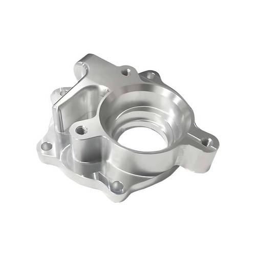
Precision Stamping Process (8 Critical Steps)
Design Engineering & DFM Analysis
CAD/CAM design of part and tooling. Design for Manufacturability (DFM) analysis to optimize part geometry for stamping. Tolerance analysis: ±0.01-0.1mm depending on part size.
Tooling & Die Design
Precision die design including: punch, die cavity, stripper plate, guide pins, and ejection system. Die material: D2 tool steel or carbide for long life. Die clearance: 10-15% of material thickness.
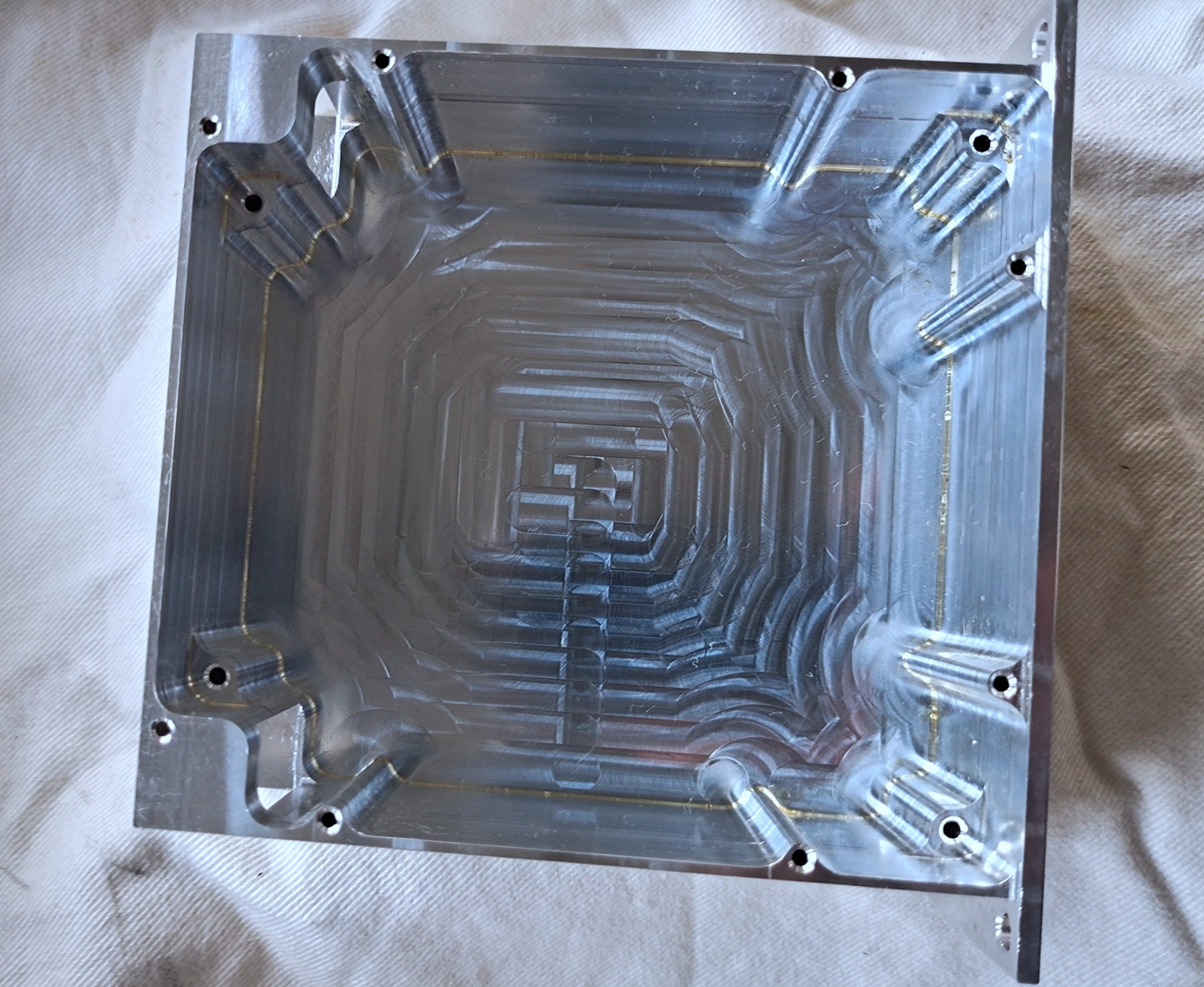
Die Manufacturing & Precision Machining
CNC machining of die components. Wire EDM for precision features (±0.002mm accuracy). Surface finish: Ra 0.2-0.4μm for die cavities. Heat treatment: HRC 58-62 for wear resistance.
Material Preparation & Blanking
Coil or sheet metal is cut to size. For progressive dies: coil stock (width 50-2000mm) with precision feeding. Material thickness: 0.1-20mm depending on press capacity.
Lubrication Application
Specialized stamping lubricants (oil-based or dry film) applied to reduce friction and prevent galling. Lubricant thickness: 5-20μm. Critical for stainless steel and high-strength alloys.
Precision Stamping Operation
Hydraulic/mechanical press applies force (20-2000 tons) to form metal. Press speed: 10-1000 strokes per minute. For progressive dies: multiple operations in single press cycle.
Part Ejection & Separation
Finished parts are ejected from die using springs, air pressure, or mechanical ejectors. Scrap is separated and collected for recycling.
Secondary Operations & Finishing
Deburring (tumbling, vibratory finishing), heat treatment (stress relieving), surface treatment (plating, painting), and quality inspection.
Material Science Deep Dive (The Nerdy Stuff That Matters)
Etching Material Compatibility Matrix
Key Material Properties for Etching:
- Corrosion Rate: Must be consistent across material surface
- Uniformity: Grain size ≤50μm for consistent etching
- Purity: ≥99.5% for predictable chemical reactions
- Surface Condition: No oxides or contaminants
Stamping Material Performance Metrics
Critical Stamping Material Properties:
- Formability: Elongation ≥15% for complex shapes
- Springback: ≤5° for dimensional accuracy
- Work Hardening: Controlled to avoid cracking
- Lubricity: Surface conditions for reduced die wear
Material Selection Decision Tree:
For thin parts (<0.3mm) with complex features: Choose etching-compatible materials (stainless steel, copper, aluminum)
For thick parts (>0.3mm) with simple shapes: Choose stamping-friendly materials (mild steel, aluminum alloys)
For high-temperature applications: Titanium or high-nickel alloys (etching recommended)
For electrical conductivity needs: Copper or brass (both processes work, etching better for precision)
Quality Control & Inspection (How We Ensure Perfection)
Etching Quality Control Protocol
Dimensional Inspection:
- Coordinate Measuring Machine (CMM): ±0.002mm accuracy, inspects 100% of critical dimensions
- Vision Systems: 2D measurement with 0.001mm resolution, 100% inspection capability
- Profile Projectors: For complex geometries, 0.005mm precision
Surface Quality Inspection:
- Surface Roughness Testers: Ra, Rz measurements (target: ≤0.8μm)
- Microscopic Inspection: 50-200x magnification for burr detection
- Cleanliness Testing: Ion chromatography for residual chemicals
Process Control:
- Etchant Concentration Monitoring: Daily testing (refractometer measurements)
- Temperature Control: ±1°C accuracy for consistent etching rates
- Exposure Energy Verification: Weekly calibration of UV equipment
Stamping Quality Control Protocol
Dimensional Inspection:
- CMM Inspection: First article inspection, ±0.005mm accuracy
- Go/No-Go Gauges: In-process inspection, quick verification
- Optical Comparators: For profile measurements, 0.002mm precision
Mechanical Properties Testing:
- Hardness Testing: Rockwell or Vickers (HRC, HV measurements)
- Tensile Testing: Ultimate tensile strength, yield strength verification
- Springback Measurement: Critical for bent parts (±1° tolerance)
Tooling Maintenance:
- Die Wear Monitoring: Daily inspection of punch and die surfaces
- Lubricant Analysis: Regular testing for contamination and effectiveness
- Press Calibration: Monthly verification of tonnage and alignment
Statistical Process Control (SPC):
Etching SPC Metrics:
- CPK ≥ 1.33 for critical dimensions
- Defect rate ≤ 0.1% (1000 PPM)
- Process capability index: 1.67 minimum
Stamping SPC Metrics:
- CPK ≥ 1.33 for critical dimensions
- Defect rate ≤ 0.2% (2000 PPM)
- Die life consistency: ±10% variation
Cost-Benefit Analysis (The Money Talk)
Total Cost of Ownership Comparison
Break-Even Analysis:
- Simple parts: Stamping becomes cost-effective at ~50,000 pieces
- Complex parts: Stamping becomes cost-effective at ~500,000 pieces
- Micro-precision parts: Etching is always more cost-effective
Production Efficiency Metrics
Cost-Saving Tips:
- For low volume: Use etching to avoid expensive tooling
- For high volume: Use stamping for simple parts, etching for complex
- For prototypes: Etching is 10-20x faster and cheaper
- For mixed volumes: Consider hybrid approach
Environmental Impact & Sustainability (Green Manufacturing)
Etching Environmental Footprint
Chemical Management:
- Chemical Usage: 5-15 liters per m² of material
- Recycling Rate: 85-95% of etchant solutions can be recycled
- Waste Treatment: Requires pH neutralization and metal precipitation
- VOC Emissions: Low (primarily from cleaning agents)
Energy & Water Usage:
- Energy Consumption: 1.5-3.0 kWh per kg of metal processed
- Water Usage: 20-40 liters per kg of metal
- Water Recycling: 70-80% of process water can be reused
- Heat Recovery: Etchant heating systems can recover 60-70% of heat
Sustainability Features:
- Material Efficiency: Minimal scrap (5-10% vs 15-30% for stamping)
- Hazardous Waste: Properly treated chemical sludge (non-toxic when processed)
- Clean Technology: Closed-loop systems available for zero discharge
- Carbon Footprint: Lower than stamping for small to medium volumes
Stamping Environmental Footprint
Resource Consumption:
- Energy Usage: 5-15 kWh per kg of metal processed
- Water Usage: 5-15 liters per kg of metal (primarily for cooling)
- Lubricant Usage: 0.5-2.0 liters per 1000 parts
- Die Material: 50-200 kg of tool steel per die set
Emissions & Waste:
- VOC Emissions: Moderate (from lubricants and cleaning)
- Noise Pollution: 85-110 dB (requires sound insulation)
- Metal Scrap: 15-30% of raw material becomes scrap
- Particulate Matter: Low (from metal cutting)
Sustainability Challenges:
- Die Manufacturing: High energy consumption for tool steel production
- Scrap Generation: Higher material waste compared to etching
- Energy Intensity: Higher electricity usage for hydraulic presses
- Maintenance Waste: Used lubricants and cleaning solvents
Sustainability Comparison:
Etching Sustainability Advantages:
- Lower material waste (90-95% material utilization)
- Lower energy consumption for small to medium production
- Closed-loop chemical recycling systems available
- No hazardous die manufacturing process
Stamping Sustainability Advantages:
- Lower per-unit energy for high-volume production
- No chemical waste management requirements
- Simpler recycling of scrap metal
- Longer tool life reduces material consumption
Technology Trends & Future Developments (What’s Next?)
Etching Technology Innovations
Advanced Etchant Formulations:
- Environmentally Friendly Etchants: Low-toxicity, biodegradable solutions
- Selective Etching: Etchants that target specific metal alloys
- Room-Temperature Etching: Eliminates energy for heating
- Self-Stopping Etchants: Automatically stop at desired depth
Process Automation & AI:
- AI Process Control: Machine learning for real-time etchant monitoring
- Automated Inspection: 100% inspection with AI defect detection
- Digital Twin Technology: Virtual process simulation
- Smart Factories: IoT-connected etching systems
New Applications:
- MEMS Manufacturing: Micro-electro-mechanical systems
- Flexible Electronics: Etching on polymer substrates
- 3D Etching: Multi-layered microstructures
- Biomedical Devices: Precision medical implants
Stamping Technology Innovations
Advanced Tooling Materials:
- Nanocoated Dies: Diamond-like carbon coatings for extended life
- Additive Manufactured Dies: 3D printed tooling for rapid prototyping
- Smart Dies: Embedded sensors for process monitoring
- Self-Lubricating Dies: Reduces lubricant requirements
Intelligent Stamping Systems:
- Adaptive Stamping: Real-time adjustment of press parameters
- Predictive Maintenance: AI-driven maintenance scheduling
- Digital Process Twins: Virtual simulation of stamping operations
- Robotic Integration: Fully automated production lines
Emerging Applications:
- Lightweighting Solutions: Advanced high-strength steels
- Electric Vehicle Components: Battery housings, motor parts
- Green Stamping: Near-net-shape processes reduce waste
- Microstamping: Precision parts for electronics
Convergence of Technologies:
The future of metal manufacturing lies in the convergence of etching and stamping technologies.
We’re seeing hybrid approaches where parts are first stamped for basic shape and then etched for precision features.
Additionally, additive manufacturing is complementing both processes for complex geometries that were previously impossible.
Sustainability will continue to drive innovation, with both processes moving toward zero-waste manufacturing models.
Digitalization and Industry 4.0 technologies will make both processes more efficient, flexible, and cost-effective.
Frequently Asked Questions (The Stuff People Actually Ask)
Q: Can etching achieve the same strength as stamping?
A: No, because etching doesn’t work-harden the material. Stamped parts have increased hardness (15-30% higher) due to plastic deformation.
If you need strength and precision, consider stamping basic shape then etching features, or use thicker material with etching.
Q: What’s the smallest feature size each process can achieve?
A: Etching can do 0.02mm features (with specialized processes), while stamping is limited to ~0.1mm minimum feature size.
For micro-precision applications (like medical devices or electronics), etching is the clear winner.
Q: Which process is better for high-volume production?
A: Stamping is faster for simple parts (1,000-10,000 parts/hour vs 50-500 for etching).
But for complex parts with many features, etching can be more efficient because it creates all features simultaneously.
The break-even point depends on part complexity and volume.
Q: Can both processes work with the same materials?
A: Mostly yes, but some materials are better suited for one process.
Titanium and high-nickel alloys are easier to etch, while high-strength steels are better for stamping.
Copper and aluminum work well with both processes.
Q: How do I decide which process to choose for my project?
A: Use this decision tree:
- If features <0.1mm or parts <0.1mm thick: Choose etching
- If production volume >1M simple parts: Choose stamping
- If you need prototypes quickly: Choose etching (3-7 days vs 4-8 weeks)
- If you need both strength and precision: Consider hybrid approach
Q: What are the typical lead times for each process?
A: Etching has much shorter lead times: 3-7 days for prototypes, 2-3 weeks for production.
Stamping requires 4-8 weeks for die manufacturing plus 1-2 weeks for production setup.
For time-sensitive projects, etching is the clear choice.
My Final Verdict (From Someone Who’s Been There)
Choose Etching If:
- You need super precision (±0.01mm or better) or micro-features (<0.1mm)
- Your parts are thin (≤0.3mm) or have complex geometries
- Design has intricate details like fine holes, slots, or patterns
- Production volume is small to medium (50-50,000 pieces)
- Material is heat-sensitive or you need to preserve original properties
- You need fast prototypes or frequent design changes
- Environmental impact is a key consideration
Choose Stamping If:
- You need high strength parts with work-hardened properties
- Your parts are thick (>0.3mm) with simple structural shapes
- Design has basic features like bends, holes, and simple cuts
- Production volume is large (>50,000 pieces)
- Cost per piece is critical and you can amortize tooling costs
- You need high production speed for simple components
- Part requires deep drawing or complex 3D forming
Pro Tip For Maximum Success:
Don’t limit yourself to just one process! Many successful manufacturers use a hybrid approach:
Example 1: Stamp the basic shape for strength, then etch the precision features
Example 2: Etch prototypes for design validation, then stamp for production
Example 3: Use etching for complex low-volume parts and stamping for simple high-volume parts in the same product
The best solution depends on your specific requirements, budget, and timeline. Always prototype first to validate your design choices!