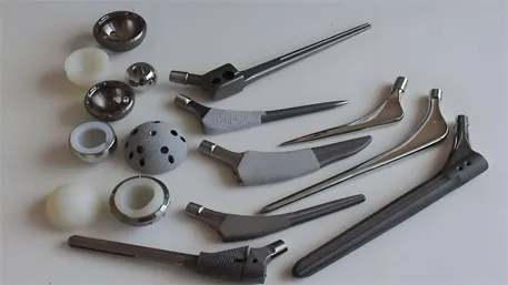
We provide ultra-precision CNC machining for semiconductor equipment components, including vacuum chambers, wafer handling parts, and gas delivery systems, with tight tolerances up to ±0.005 mm and strict contamination control. With 26 years of precision manufacturing experience serving the semiconductor supply chain, we help OEMs and equipment manufacturers meet the strictest industry requirements for purity, precision, and reliability.
Semiconductor Equipment Components We Machine
We specialize in manufacturing high-precision components for critical semiconductor manufacturing equipment, covering all core process modules:
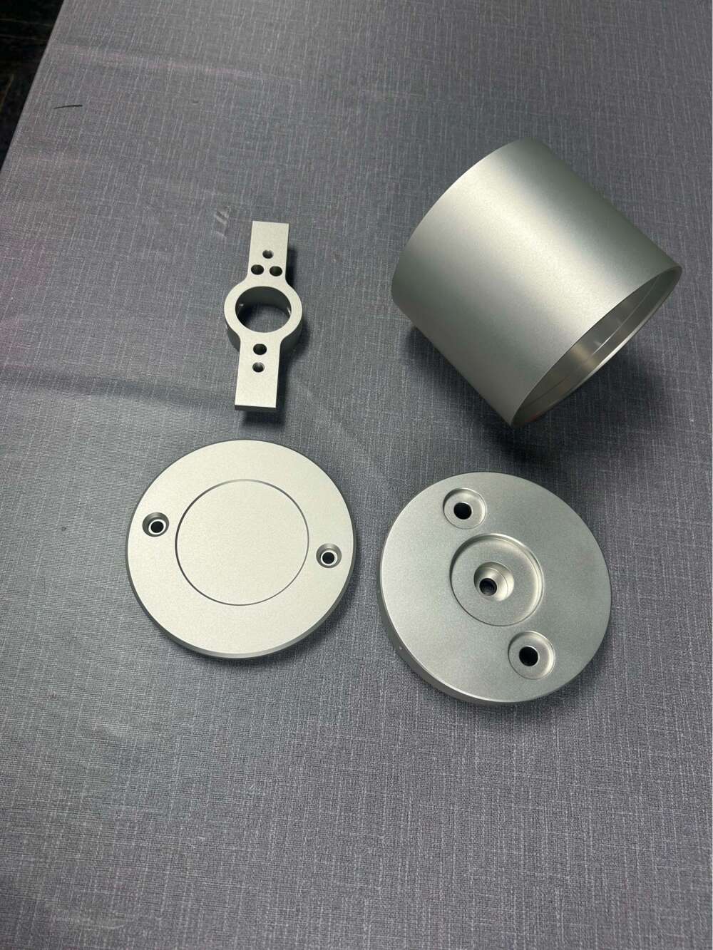
- Vacuum chamber components & vacuum flanges
- Wafer handling arms & robotic end effectors
- Gas delivery system parts & flow components
- Electrostatic chuck (ESC) base components
- Precision alignment fixtures & positioning stages
- Process kit parts & chamber liners
- High-purity fluid handling components
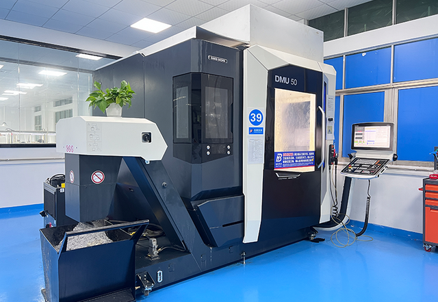
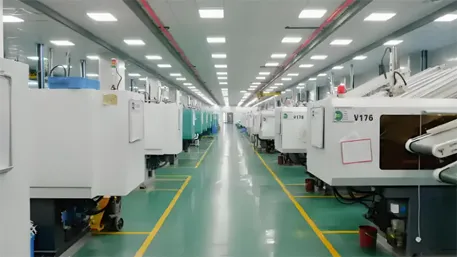
Key Machining Capabilities
Our advanced 5-axis CNC machining centers and precision process control enable us to meet the ultra-strict requirements of semiconductor manufacturing. All parameters are verified through thousands of production runs:
| Item | Specification |
|---|---|
| Precision Tolerance | ±0.005 mm (Standard) / ±0.003 mm (Ultra-precision option) |
| Surface Roughness | Ra 0.2 μm (Standard) / Ra 0.05 μm (Ultra-smooth option) |
| Maximum Part Size | 1000 x 800 x 500 mm |
| Minimum Feature Size | 0.01 mm |
| Cleanroom Class | Class 100 / ISO 5 |
Materials for Semiconductor Parts
We only source high-purity raw materials certified for semiconductor applications, with strict outgassing and corrosion resistance properties to meet vacuum and clean environment requirements:
Aluminum Alloys (6061-T6 / 7075-T6)
The most common material for vacuum chambers and structural parts. 6061 offers excellent thermal conductivity and corrosion resistance, while 7075 provides higher strength for load-bearing components. Both feature low outgassing properties ideal for vacuum environments.
316L Stainless Steel
Ultra-low carbon stainless steel with exceptional corrosion resistance against corrosive process gases. Ideal for gas delivery systems and corrosive environment components. Electropolished finish ensures minimal particle generation.
High-Purity Plastics (PEEK / PTFE)
High-purity engineering plastics with excellent electrical insulation and chemical resistance. Extremely low outgassing, making them ideal for insulator components and fluid handling parts in wet process tools.
Titanium & Ceramics
Titanium offers high strength-to-weight ratio and corrosion resistance for wafer handling parts. Alumina ceramics provide excellent insulation and wear resistance for electrostatic chuck components and high-temperature process parts.
Surface Finishing Options
All our surface finishes comply with semiconductor contamination control standards, ensuring minimal particle generation and maximum corrosion resistance:
Hard Anodizing
Enhances corrosion and wear resistance, provides non-conductive surface for aluminum parts.
Electropolishing
Creates ultra-smooth, passivated surface for stainless steel, reducing particle adhesion.
Passivation
Chemical treatment to remove free iron from stainless steel surfaces, enhancing corrosion resistance.
PTFE Coating
Non-stick, low-friction coating with excellent chemical resistance for process components.
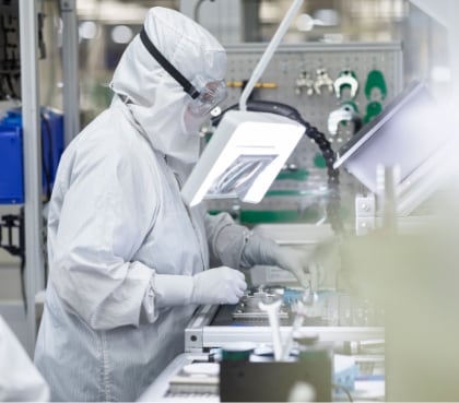
Cleanroom & Contamination Control
Contamination control is the most critical requirement for semiconductor parts. Our specialized cleanroom manufacturing process eliminates particle, residue, and outgassing risks that could damage your wafer processing:
- Multi-stage Ultrasonic Cleaning: Removes machining residue and micro-particles from part surfaces and internal channels.
- DI Water Rinse: Deionized water rinse to eliminate ionic contamination, ensuring no residual contaminants.
- Particle Inspection: Automated particle counting to verify surface cleanliness before packaging.
- Class 100 Cleanroom Packaging: Parts are cleaned, inspected, and packaged in ISO 5 cleanroom environment to prevent re-contamination during shipping.
Challenges in Semiconductor CNC Machining & Our Solutions
Conclusion: CNC machining is the preferred method for semiconductor equipment parts requiring ultra-high precision and contamination control. With 20 years of experience, we have developed specialized solutions to overcome the unique challenges of semiconductor manufacturing:
| Manufacturing Challenge | Our Solution |
|---|---|
| Micron-level tolerance requirement | 5-axis CNC machining + real-time thermal compensation system to maintain precision in temperature-controlled workshop |
| Surface contamination risk | Multi-stage cleaning process + cleanroom packaging, with full cleanliness verification before delivery |
| Material deformation after machining | Stress relief machining process + precision fixturing to eliminate residual stress and part deformation |
| High purity requirement | Full material traceability system, with material certification and outgassing test report available |
Quality Assurance & Traceability
We implement strict quality control processes to ensure every part meets your exact specifications, with full documentation to support your supply chain qualification:
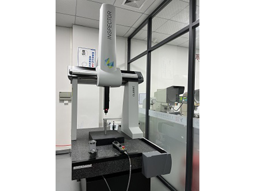
- Coordinate Measuring Machine (CMM) dimensional inspection for 100% critical dimensions
- Surface roughness testing to verify finish requirements
- Full material certification with batch traceability
- Cleanliness verification test to ensure no residual contamination
- First Article Inspection (FAI) report for new projects
- Full part traceability available for all production batches
What Affects the Cost of Semiconductor Parts?
Transparent cost breakdown to help you plan your project budget. We optimize your design to reduce cost while maintaining all performance requirements:
Material Grade
High-purity materials for semiconductor applications have different cost levels. We help you select the most cost-effective material that meets your performance needs.
Tolerance Requirement
Tighter tolerances require more precise machining and inspection, which affects cost. Our engineers can help optimize tolerance where possible.
Surface Finishing
Different finishing options have different costs. We recommend the most suitable finish based on your application environment.
Cleanroom Requirement
Cleanroom processing and packaging adds cost but is essential for semiconductor applications. We offer flexible options based on your needs.
Compliance & Industry Standards
All our processes and products comply with international semiconductor industry standards to support your supply chain qualification and regulatory compliance:
ISO 14644-1
Cleanroom air cleanliness classification standard, ensuring our Class 100 cleanroom meets the strictest particle control requirements.
ASTM E595
Standard test method for outgassing in vacuum environment, ensuring our materials meet low outgassing requirements for vacuum systems.
SEMI Standards
Semiconductor Equipment and Materials International standards, ensuring our products comply with semiconductor industry specifications.
ISO 9001:2015
Quality management system certification, ensuring consistent process control and product quality for all production batches.
Quality Testing Data (Data for reference only)
We conduct rigorous internal testing to verify the performance of our semiconductor parts. Below are typical test results from our laboratory:
| Test Item | 6061 Aluminum (Anodized) | 316L Stainless Steel | PEEK |
|---|---|---|---|
| ASTM E595 Outgassing TML | <0.2% (Pass) | <0.1% (Pass) | <0.5% (Pass) |
| ASTM E595 Outgassing CVCM | <0.05% (Pass) | <0.01% (Pass) | <0.08% (Pass) |
| Surface Particle Count (>0.1μm) | <100 particles / cm² | <80 particles / cm² | <120 particles / cm² |
| Neutral Salt Spray Test | 1000+ hours (No corrosion) | 2000+ hours (No corrosion) | N/A |
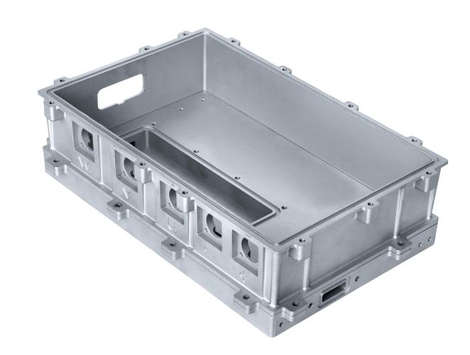
Case Study: Vacuum Chamber Component for Wafer Processing Equipment
Client
Leading Global Wafer Etching Equipment OEM
Part
6061 Aluminum Vacuum Chamber Body
Tolerance Requirement
±0.003 mm
Surface Treatment
Hard Anodizing + Cleanroom Cleaning
Order Quantity
200 pcs / year
We delivered high-precision aluminum vacuum chamber components for a leading semiconductor equipment manufacturer. The parts required ultra-tight tolerance to ensure vacuum sealing, plus cleanroom processing to eliminate contamination risks. All parts passed 1000-hour outgassing test and full FAI inspection, helping our client qualify for the global top 3 semiconductor OEM supply chain.
Frequently Asked Questions
What tolerance is required for semiconductor equipment parts?
Most semiconductor parts require tolerances between ±0.005 mm to ±0.003 mm to ensure proper fit and function in vacuum and precision processing environments. We can achieve even tighter tolerances for ultra-precision applications.
What materials are best for vacuum environments in semiconductor tools?
Aluminum alloys (6061/7075) and 316L stainless steel are the most common materials for vacuum environments, due to their low outgassing properties and excellent corrosion resistance. For high-temperature applications, titanium and ceramics are also widely used.
How do you prevent contamination during manufacturing?
We implement a full contamination control process: multi-stage ultrasonic cleaning with DI water, particle inspection, and final packaging in Class 100 cleanroom environment. This ensures no particles, residue, or ionic contamination is left on the parts.
Do you provide cleanroom packaging for semiconductor parts?
Yes, all semiconductor parts are cleaned, inspected, and double-bagged in our ISO 5 cleanroom to prevent re-contamination during shipping. We can also provide custom packaging based on your specific requirements.
Can you support new product qualification for the semiconductor supply chain?
Yes, we have extensive experience supporting supplier qualification for major semiconductor OEMs. We can provide all required documentation, including material certificates, test reports, FAI reports, and process documentation to support your qualification process.
Ready to Get Your Custom Semiconductor Parts?
Get a free quote within 24 hours, plus free DFM review to optimize your design for manufacturability.